

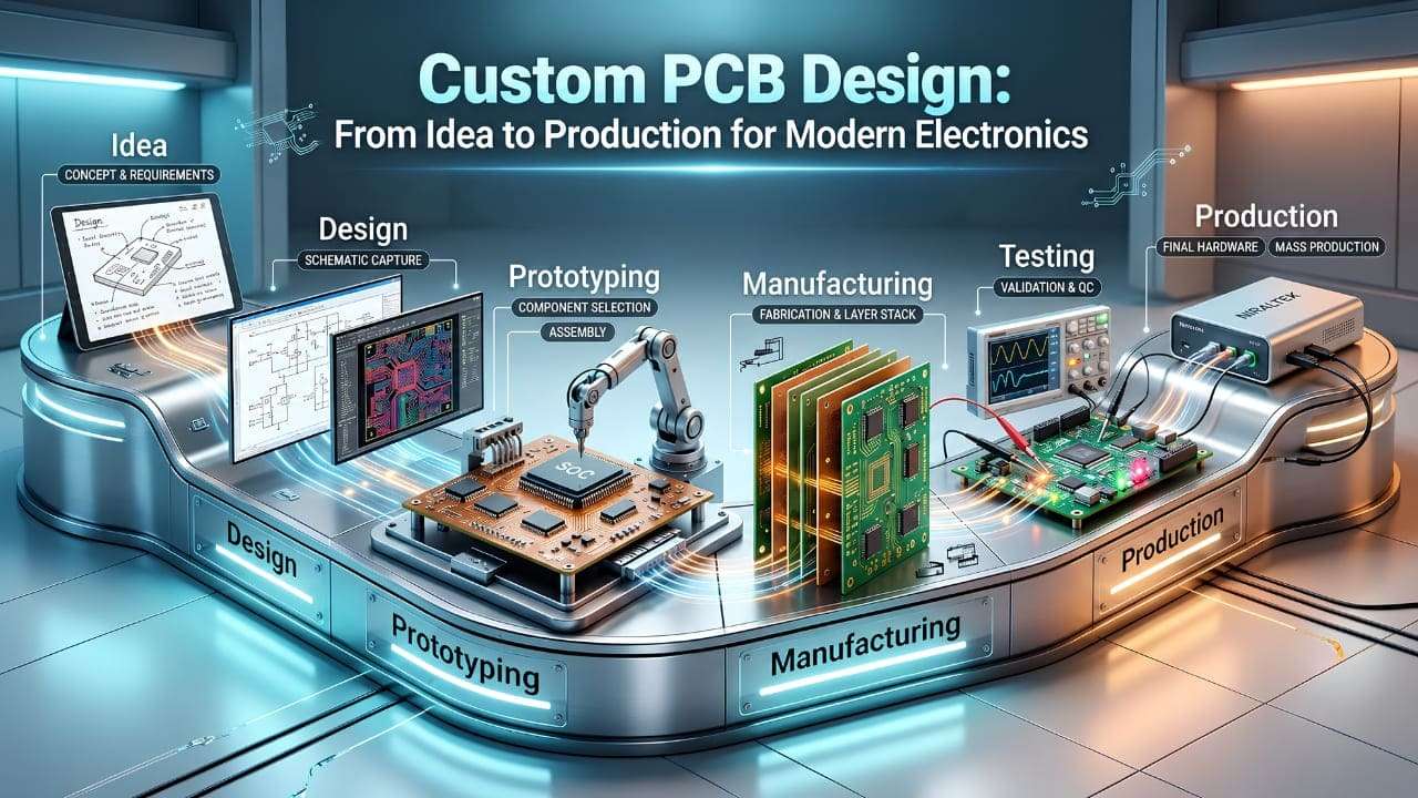
Every successful electronic product begins with custom PCB design. Whether you’re developing an IoT gateway, industrial controller, medical device, or embedded system, the PCB directly impacts signal integrity, thermal performance, manufacturability, and long-term reliability. According to manufacturing research, 70–80% of a product’s manufacturing cost is determined during the design phase, making early engineering decisions critical for quality and cost optimization.
Why custom PCB design matters
- Improves signal integrity and electrical performance
- Reduces prototype revisions and manufacturing defects
- Enhances thermal management and product reliability
- Accelerates the journey from idea to production-ready hardware
What Is Custom PCB Design?
Custom PCB Design is the process of creating a printed circuit board specifically for a product’s electrical, mechanical, and manufacturing requirements. Unlike standard or off-the-shelf boards, a custom PCB is engineered to match the exact functionality, size, power consumption, and performance goals of an electronic device.
According to industry manufacturing studies, 40–80% of the total PCBA cost comes from component selection and design decisions, making early PCB engineering one of the most important stages of product development.
Why businesses choose custom-made PCB design Boards
- Fits unique product dimensions and hardware architecture
- Increase profit margins by manufacturing your own branded hardware instead of reselling third-party products.
- Offer flexible pricing and distributor discounts without depending on another supplier’s pricing model.
- Own your product design and OEM branding, giving your business complete control over the hardware.
- Reduce supplier dependency and avoid business disruptions if a third-party manufacturer discontinues the product.
- Scale confidently from prototype to production while maintaining consistent quality and supply.
Custom PCB vs Standard PCB
| Feature | Custom PCB | Standard PCB |
| Design | Tailored for one product | Generic layout |
| Performance | Optimized for application | Limited flexibility |
| Scalability | Prototype to mass production | Best for basic projects |
| Example | IoT gateway, medical device | Arduino shield, demo board |
The Custom PCB Design Process
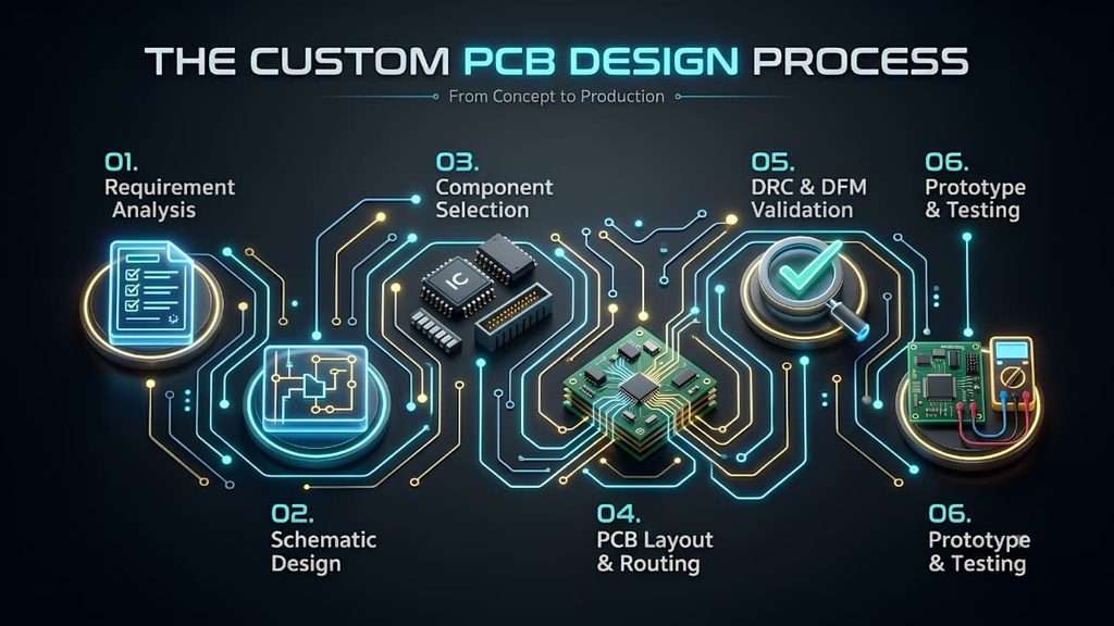
A successful Custom PCB Design project follows a structured engineering process that transforms an idea into a production-ready electronic product. Each stage improves performance, reduces manufacturing risks, and minimizes costly redesigns.
Step-by-step workflow
- Requirement Analysis: Define product size, power needs, interfaces, and functionality.
- Schematic Design: Create the electrical circuit and select suitable components.
- Component Selection: Choose reliable ICs, connectors, sensors, and power modules.
- PCB Layout & Routing: Optimize trace routing, grounding, and signal integrity.
- DRC & DFM Validation: Verify design rules and manufacturability before fabrication.
- Prototype & Testing: Build the first PCB, validate performance, and prepare for production.
Example
A smart energy monitoring device begins with sensor requirements, followed by schematic design, PCB layout, prototype testing, and finally mass production. Before moving to fabrication, engineers verify the design using IPC Design Standards to improve manufacturability, quality, and production reliability.
PCB Layout Best Practices for Reliable Hardware
A reliable electronic product depends on a well-planned PCB layout. Good layout practices improve signal integrity, reduce electrical noise, manage heat efficiently, and prepare the board for manufacturing. Engineers who optimize the layout early often avoid costly prototype revisions later.
Best practices every hardware engineer should follow
- Place components strategically: Keep processors, memory, and sensors close to related circuits.
- Maintain short signal traces: Reduce latency and improve high-speed communication.
- Use a continuous ground plane: Minimize EMI and stabilize return current paths.
- Optimize power routing: Use wider copper traces for high-current circuits.
- Plan thermal management: Add thermal vias and copper areas around power components.
Single-Layer vs Multi-Layer PCB Design
Choosing the right PCB structure depends on your product’s complexity, performance, and manufacturing requirements. Single-layer PCBs work well for simple electronic circuits, while multi-layer PCBs support compact, high-speed, and feature-rich devices such as IoT gateways and industrial controllers.
Key differences
| Feature | Single-Layer PCB | Multi-Layer PCB |
| Copper Layers | 1 | 2+ layers |
| Complexity | Simple circuits | Advanced electronics |
| Cost | Lower | Higher |
| Best For | LED boards, power supplies | IoT, medical & industrial devices |
When should you choose each?
- Choose single-layer: Basic consumer electronics and low-complexity control boards.
- Choose multi-layer: Embedded systems, communication devices, and high-speed PCB applications.
Example: A smart energy monitoring system uses a multi-layer PCB to separate power, signal, and ground layers, improving reliability, reducing EMI, and enabling a compact hardware design.
Common Mistakes in Custom PCB Design
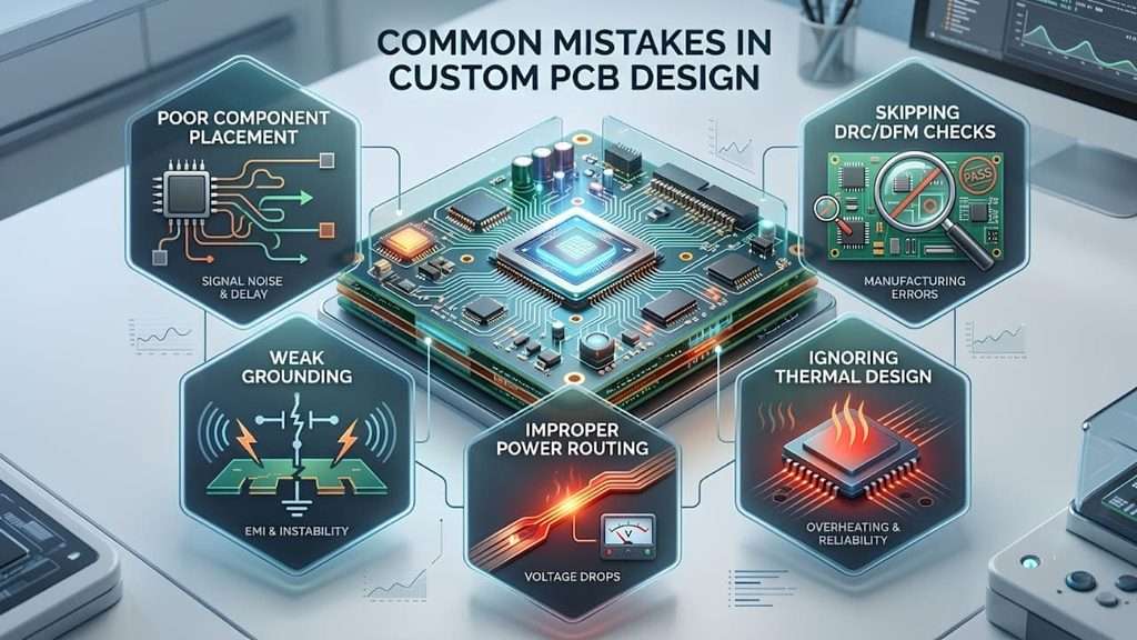
Even experienced engineers can make PCB design mistakes that affect product performance, reliability, and manufacturing. Identifying these issues early helps reduce prototype failures, save development time, and improve production quality.
Mistakes to avoid
- Poor component placement: Long routing paths increase signal delay and electrical noise.
- Weak grounding: An incomplete ground plane can create EMI and unstable circuit performance.
- Improper power routing: Narrow power traces may cause voltage drops during high-current operation.
- Ignoring thermal design: Missing thermal vias or copper balancing can lead to overheating.
- Skipping DRC and DFM checks: Manufacturing errors often appear when engineers ignore design rule validation.
Industries Using Custom PCB Design
Custom PCB Design powers modern electronics across industries that demand high reliability, compact hardware, and long-term performance. Instead of using generic circuit boards, businesses design PCBs to match their exact product requirements, operating conditions, and manufacturing goals.
Where custom PCB design is used
- Industrial Automation: PLCs, motor controllers, and machine monitoring systems require durable, high-performance PCBs.
- IoT & Smart Devices: Smart sensors, IoT gateways, wearables, and connected home devices rely on compact multi-layer PCB designs.
- Medical Electronics: Patient monitoring equipment and diagnostic devices need low-noise, highly reliable circuit boards.
- Smart Energy Systems: Energy meters, solar monitoring units, and battery management systems require accurate power and signal routing.
- Consumer Electronics: Smart appliances, handheld devices, and gaming accessories use custom PCBs for smaller form factors.
Example
A smart factory IoT gateway combines Ethernet, Wi-Fi, sensors, and power management on a single custom PCB, creating a reliable and production-ready hardware platform for industrial automation.
How to Choose the Right PCB Design Partner
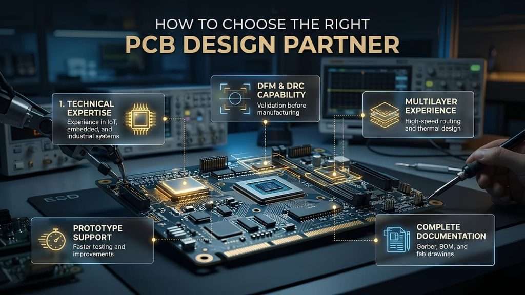
Selecting the right PCB design partner can determine whether your product reaches the market smoothly or faces repeated redesigns. A reliable engineering team should understand electronics, manufacturability, and product development—not just PCB layout.
What to look for in a PCB design partner
- Technical expertise: Experience with IoT, embedded systems, and industrial electronics.
- DFM & DRC capability: Ability to validate designs before manufacturing.
- Prototype support: Faster testing and design improvements before mass production.
- Multi-layer PCB experience: Knowledge of high-speed routing, power integrity, and thermal design.
- Complete documentation: Gerber files, BOM, Pick-and-Place, and fabrication drawings.
Ready to build reliable hardware? Explore Niraltek’s Custom PCB Design services and turn your idea into a production-ready electronic product.
Conclusion
Custom PCB Design transforms innovative ideas into reliable, production-ready electronic products. From schematic design and PCB layout to DFM validation, prototyping, and manufacturing, every engineering decision influences product performance, cost, and long-term reliability.
Whether you’re developing an IoT device, industrial automation system, medical electronics, or embedded hardware, investing in the right PCB design process helps reduce redesigns and accelerate time-to-market.
Frequently Asked Questions (FAQs)
1. What does PCB stand for in electronics?
PCB stands for Printed Circuit Board. It is the foundation of an electronic device that connects components, distributes power, and enables reliable communication between circuits.
2. What is the difference between custom PCB design and a standard PCB?
A custom PCB is engineered for a specific product’s size, functionality, and performance requirements, while a standard PCB uses a generic layout suitable for basic or off-the-shelf applications.
3. When should a business choose a custom PCB?
Choose a custom PCB when developing IoT devices, industrial automation systems, medical electronics, smart energy products, or any hardware that requires compact design and reliable performance.
4. What is DFM in PCB design?
DFM stands for Design for Manufacturing. It ensures that the PCB layout follows manufacturing guidelines, helping reduce fabrication errors, improve production quality, and minimize redesign costs.
5. What files are required before PCB manufacturing?
A production-ready PCB typically requires Gerber files, Bill of Materials (BOM), NC Drill files, Pick-and-Place files, and assembly drawings to support accurate fabrication and assembly.
6. How long does a custom PCB design project usually take?
The timeline depends on product complexity. A simple PCB may take a few days, while multi-layer or embedded hardware projects typically require additional time for schematic design, layout, prototyping, and validation.