

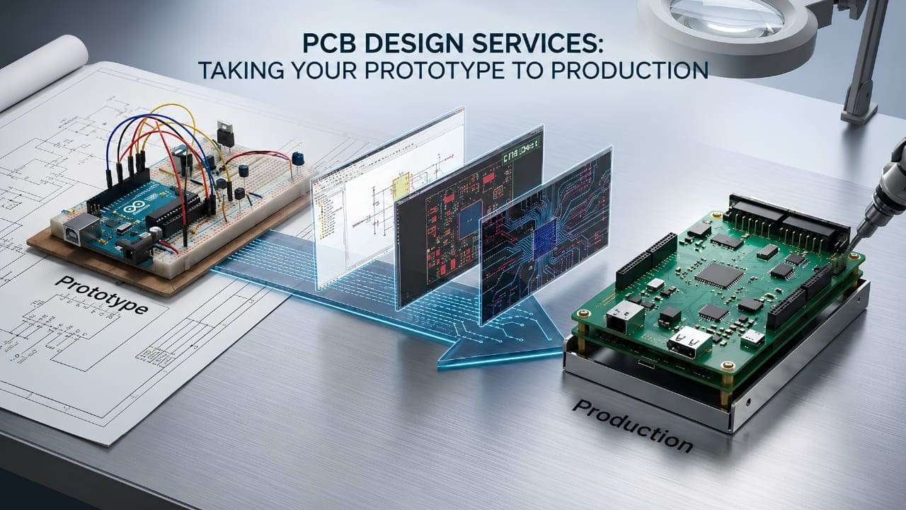
A PCB prototype may work on the bench, but that does not always mean it is ready for production. Poor component selection, routing, thermal management, or manufacturing considerations can create costly redesigns and failures. IPC reports that up to 70% of electronics product failures can be traced to design flaws, highlighting the importance of getting PCB design right from the beginning.
Professional PCB Design Services help businesses turn product concepts into reliable, production-ready electronics through:
- Custom PCB design and layout
- Hardware design and development
- Power, signal, and thermal considerations
- DFM and DFT reviews
- Prototype testing and validation
- Prototype-to-production support
The right approach connects ideas to products while reducing design risks, unnecessary iterations, and manufacturing challenges.
What Are PCB Design Services?
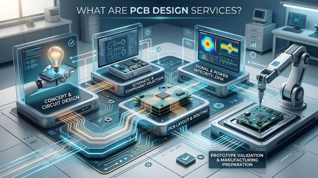
PCB Design Services help turn an electronic concept or circuit into a functional, manufacturable printed circuit board. The process covers electrical design, component selection, PCB layout, routing, validation, and preparation for manufacturing.
IPC reports that up to 70% of electronics product failures can trace back to design flaws, while standardized design practices can reduce manufacturing defects by 20–40%.
A professional PCB design process typically includes:
- Schematic and circuit design
- Component and footprint selection
- PCB placement and routing
- Power and signal integrity checks
- DFM and DFT reviews
- Prototype validation and production preparation
| Requirement | Example |
| Compact product | Wearable device PCB |
| Connectivity | IoT gateway with Wi-Fi and Ethernet |
| Power management | Industrial control board |
| Production readiness | DFM-checked Custom PCB |
PCB Design Services Workflow
A professional PCB Design Services workflow ensures every stage of development is optimized for performance, manufacturability, and production readiness. From the initial concept to prototype validation, each step helps reduce design risks and speed up product development.
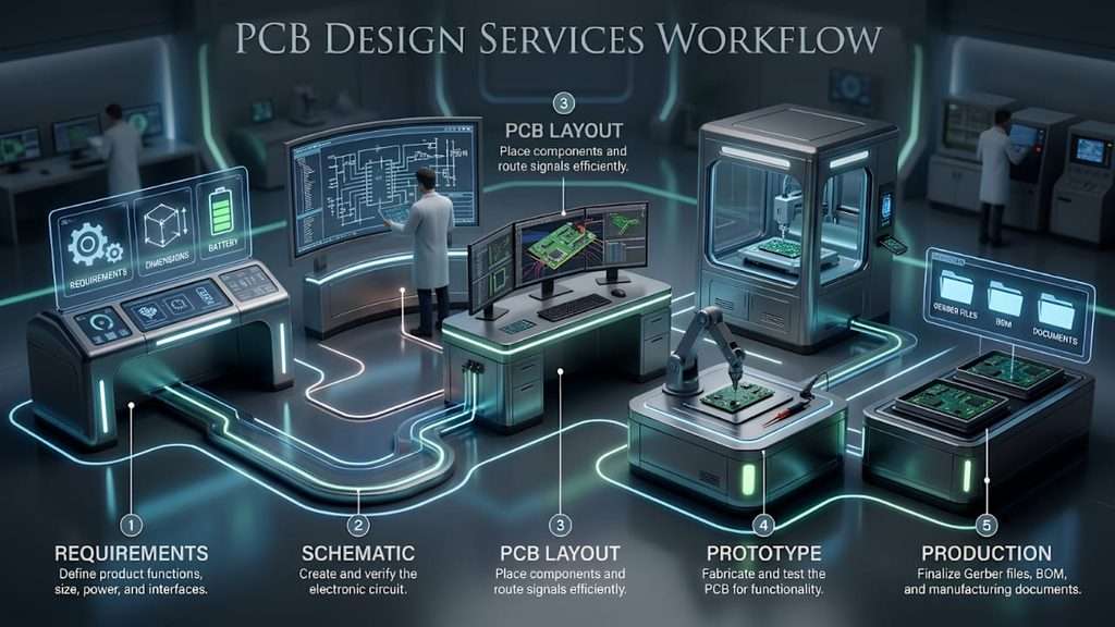
- Requirements: Define product functions, size, power, and interfaces.
- Schematic: Create and verify the electronic circuit.
- PCB Layout: Place components and route signals efficiently.
- Prototype: Fabricate and test the PCB for functionality.
- Production: Finalize Gerber files, BOM, and manufacturing documents.
From Idea to Product: The PCB Design Process
Turning an electronics idea into a working product requires more than drawing a circuit. A structured PCB design process helpsengineers move from requirements to a validated, manufacturable board. IPC’s design flow includes schematic capture, component placement, routing, design-rule checks, documentation, and final review.
The process typically follows these steps:
- Define requirements: Identify functions, power, size, interfaces, and operating conditions.
- Create the schematic: Build and verify the electrical circuit.
- Design the layout: Place components and route connections while considering signal, power, thermal, and mechanical constraints.
- Review and validate: Run design checks and verify performance through prototyping.
- Prepare for production: Generate manufacturing documentation and release the design.
7 Common PCB Design Mistakes to Check Before Production
A PCB can pass initial testing and still create problems during manufacturing. A proper pre-production review helps catch issues before they become expensive redesigns. IPC notes that design flaws can account for up to 70% of electronics product failures, while DFM helps identify manufacturing risks early.
Before releasing your Custom PCB, check these seven areas:
- Incorrect component footprints: Verify every footprint against the actual component.
- Poor component placement: Maintain adequate clearance for assembly and testing.
- Insufficient trace width: Match trace widths to current and manufacturing requirements.
- Weak power and grounding: Check power distribution, return paths, and decoupling.
- Signal integrity issues: Review high-speed and sensitive signal routing.
- Manufacturing constraints: Confirm clearances, holes, stack-up, and fabrication capabilities.
- Incomplete documentation: Verify Gerber files, drill files, BOM, and assembly data.
PCB Design vs DFM vs DFT: What Is the Difference?
PCB Design, Design for Manufacturing (DFM), and Design for Testability (DFT) solve different problems, but they work together to create a production-ready board. IPC describes DFM as a process that helps ensure a design can be manufactured consistently with minimal defects.
- PCB Design: Engineers create the schematic, select components, place parts, and route connections.
- DFM: Engineers check whether manufacturers can build the PCB reliably using available processes and capabilities.
- DFT: Engineers make the board easier to inspect, test, and troubleshoot. IPC includes testability as a key part of electronics design review.
How PCB Design Handles Power, RF and Mechanical Constraints
Professional PCB Design Services help create a reliable Custom PCB that balances electrical performance with RF and mixed-signal PCB layout guidelines. Engineers consider these constraints early because they directly affect routing, component placement, signal quality, and manufacturability. IPC board-design standards specifically address electrical integrity, signal and power performance, and physical design requirements.
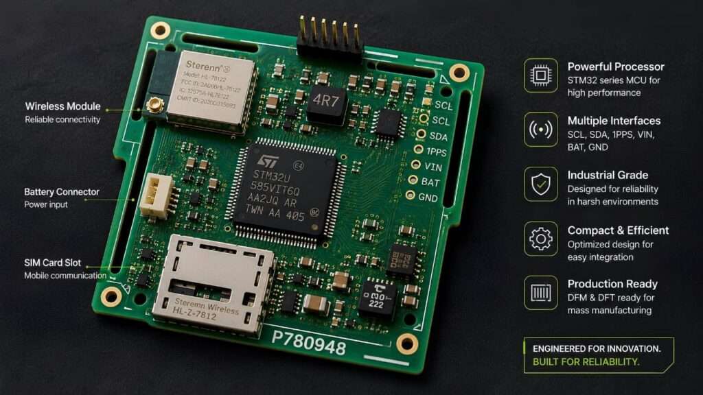
Key considerations include:
- Power: Engineers plan power distribution, grounding, trace widths, and decoupling to support stable operation.
- RF: Engineers control impedance, trace length, grounding, and signal paths to reduce noise and signal loss.
- Mechanical: Engineers match the PCB to the enclosure, connectors, mounting holes, component height, and thermal requirements.
From Development Board to Custom Production PCB
A development board helps engineers test an idea quickly, but it rarely fits the final product’s size, cost, power, and functionality requirements.Moving to a Custom PCB through professional PCB Design Services lets teams optimize the design around the actual product.
The transition usually involves:
- Validate the concept: Use a development board to test firmware, sensors, communication, and core functions.
- Define product requirements: Identify size, power, interfaces, components, and production volume.
- Create the Custom PCB: Integrate the required circuits, connectors, power management, and communication features.
- Optimize for production: Review component availability, manufacturability, testing, thermal performance, and assembly.
- Prototype and validate: Build prototype boards, test performance, fix issues, and prepare manufacturing files.
How PCB Design Fits Into Hardware Development Services
PCB Design Services forms a core part of Hardware Development Services because it connects the electronic concept with a functional product. A good hardware development process does not treat the PCB as an isolated task. Engineers align the board with the product’s electrical, mechanical, firmware, and manufacturing requirements from the start.
The process typically includes:
- Requirement analysis: Define product functions, power needs, interfaces, size, and operating conditions.
- Circuit development: Select components and create the schematic around the product requirements.
- PCB design: Place components, route signals, manage power, and address thermal and mechanical constraints.
- Prototype development: Build and test the board to identify design issues early.
- Validation: Check functionality, performance, reliability, and product-specific requirements.
- Production preparation: Optimize the design for manufacturing, assembly, testing, and scalability.
How PCB Design Supports Electronics Product Development
PCB Design Services play an important role in Electronics Product Development by turning product requirements into practical electronic hardware. Instead of designing the board separately, engineers align the PCB with the product’s functionality, size, power, connectivity, and manufacturing goals from the beginning.
A well-planned PCB design can help teams:
- Translate requirements into hardware: Convert product functions into circuits, components, and interfaces.
- Optimize product size: Integrate multiple functions onto a compact Custom PCB.
- Improve reliability: Address power, thermal, signal integrity, and component requirements during design.
- Reduce development iterations: Identify potential design issues before manufacturing.
- Prepare for production: Consider DFM, DFT, component availability, assembly, and testing requirements.
- Support product scalability: Create a design that can adapt to future product versions or production volumes.
What Should You Share With a PCB Design Partner Before Starting?
A PCB design project starts smoothly when you provide the right information upfront. Clear requirements help engineers understand your product, select suitable components, plan the board architecture, and avoid unnecessary design changes later.
Before starting your PCB Design Services project, share:
- Product requirements: Explain the product’s purpose, key functions, and expected operating conditions.
- Circuit or block diagram: Provide existing schematics, reference designs, or a functional block diagram if available.
- Power requirements: Mention input voltage, current requirements, battery specifications, and power constraints.
- Components: Share preferred components, approved parts, or existing BOMs.
- Connectivity: Specify interfaces such as USB, Ethernet, CAN, RS-485, Wi-Fi, or Bluetooth.
- Mechanical details: Provide PCB dimensions, enclosure drawings, mounting holes, connector locations, and height restrictions.
- Production requirements: Mention expected production volume, target cost, testing needs, and manufacturing preferences.
- Existing prototypes: Share development-board designs, test results, or previous PCB versions.
How to Choose the Right PCB Design Services Provider
Choosing a PCB Design Services provider involves more than checking design software or pricing. You need a partner who understands electrical, mechanical, manufacturing, testing, and reliability requirements. Look for a team that can support your project from initial design and prototyping through validation and production preparation. IPC’s DFX guidelines recommend a multidisciplinary approach covering manufacturability, assembly, testability, cost, and reliability.
Look for these factors:
- Technical expertise: Check experience with your PCB type, application, and complexity.
- Design process: Ask how the team handles schematic review, layout, DFM, DFT, and validation.
- Prototype support: Confirm whether they can support testing and design iterations.
- Production readiness: Check their approach to BOMs, Gerbers, assembly, and manufacturing documentation.
- Industry experience: Review relevant projects and technical case studies.
| What to Check | Example |
| Design expertise | High-speed or RF PCB experience |
| DFM/DFT | Manufacturing and test reviews |
| Documentation | Gerber, BOM, drill files |
| Production support | Prototype-to-production capability |
Benefits of Professional PCB Design Services
Professional PCB Design Services help businesses turn electronic concepts into reliable, manufacturable products. An experienced design team looks beyond basic routing and considers electrical performance, thermal behavior, mechanical fit, testing, and manufacturing requirements from the start.
Key benefits include:
- Faster product development: A structured process helps teams move from concept to prototype efficiently.
- Fewer design iterations: Early design reviews can identify component, routing, power, and manufacturing issues before fabrication.
- Better reliability: Engineers evaluate signal integrity, power distribution, thermal performance, and component selection.
- Optimized Custom PCB: Teams can integrate product-specific functions while reducing unnecessary components and connections.
- Production readiness: DFM and DFT checks help prepare the board for manufacturing, assembly, and testing.
- Cost optimization: Early component and manufacturing decisions can help control development and production costs.
- Scalable designs: Engineers can prepare the PCB for future product versions and higher production volumes.
Whether you’re refining a prototype or developing a new electronic product, our PCB Design Services can support Custom PCB Design, hardware development, validation, and production preparation.
Conclusion
Taking an electronics product from idea to production requires more than creating a working PCB prototype. It involves careful circuit design, component selection, layout, testing, and manufacturing preparation. Professional PCB Design Services help address power, RF, thermal, mechanical, DFM, and DFT requirements throughout the development process. By identifying design issues early and validating the prototype before production, businesses can reduce redesigns, improve reliability, and create hardware that is ready to scale. A well-planned PCB design ultimately provides a strong foundation for turning an electronics concept into a reliable, production-ready product.
Frequently Asked Questions
1. How do I know if my PCB design is ready for production?
A working prototype does not always mean production readiness. The design should pass electrical, mechanical, thermal, DFM, and DFT checks and include complete manufacturing documentation.
2. How do I know if my PCB Design Services project is ready for production?
Yes. A development board can help validate the concept before moving to a custom board designed around the product’s size, functionality, power, and production requirements.
3. What information should I provide before starting PCB Design Services?
Share your product requirements, schematics or block diagrams, power specifications, preferred components, board dimensions, enclosure details, interfaces, and expected production volume.
4. How can I reduce PCB redesigns before manufacturing?
Start design reviews early and check component footprints, routing, power distribution, thermal requirements, mechanical constraints, DFM, and DFT before releasing manufacturing files.
5. Can PCB Design Services support prototype-to-production development?
Yes. Engineers can design the board with manufacturing, testing, component availability, and scalability in mind from the prototype stage.
6. What is the difference between a development board and a custom PCB?
A development board provides a ready-made platform for testing. A custom PCB combines only the required components and functions, allowing better control over size, cost, performance, and product integration.
7. How long do PCB Design Services usually take?
The timeline depends on factors such as circuit complexity, board layers, component count, interfaces, testing requirements, and the number of design iterations.